Background:
In recent years, graphene-integrated waveguides (GIWGs) have made substantial progress in many aspects such as material preparation, device structure design, integration process to application, etc., but there are still many challenges in the process of shifting from basic research to practical applications. Therefore, systematically exploring the preparation methods of graphene integrated waveguides of different structures and establishing their structure-activity relationship with device performance will be conducive to clarifying the development direction of GIWGs and promoting their industrialization development.
Results:
In this paper, the research progress of the preparation method, performance and application of GIWGs in recent years is systematically summarized. Focusing on the preparation technology of GIWGs and their influence on device performance, four preparation methods are introduced, namely mechanical peeling, liquid phase synthesis, chemical vapor deposition (CVD) growth and transfer in situ growth without transfer, which reveals the regulation of device performance indicators by various preparation technologies, and points out the challenges and future development directions in the field of GIWGs.

Figure I. Preparation, performance and application of graphene integrated waveguides
Text guide:
Integrating graphene into the waveguide can improve its function, enhance the interaction between light and material, and improve the performance of graphene optoelectronic devices. This paper first introduces the strange photoelectric properties of graphene, including the linear optical absorption, photo-thermoelectric effect, saturable absorption, optical Kerr effect, third-order nonlinearity, four wave mixing and two-photon absorption of graphene. On this basis, the interaction mechanism between light and graphene in GIWGs structure is analyzed, showing the great development potential of GIWGs in optical communication, optical sensing and other application fields.

Figure 2. Photoelectric properties of graphene and the interaction mechanism between light and matter in GIWGs.
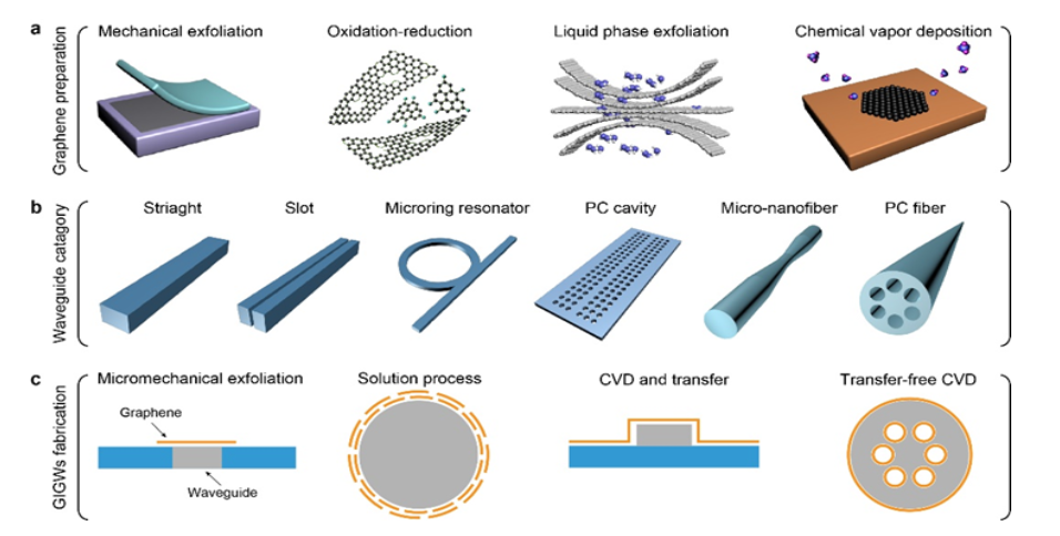
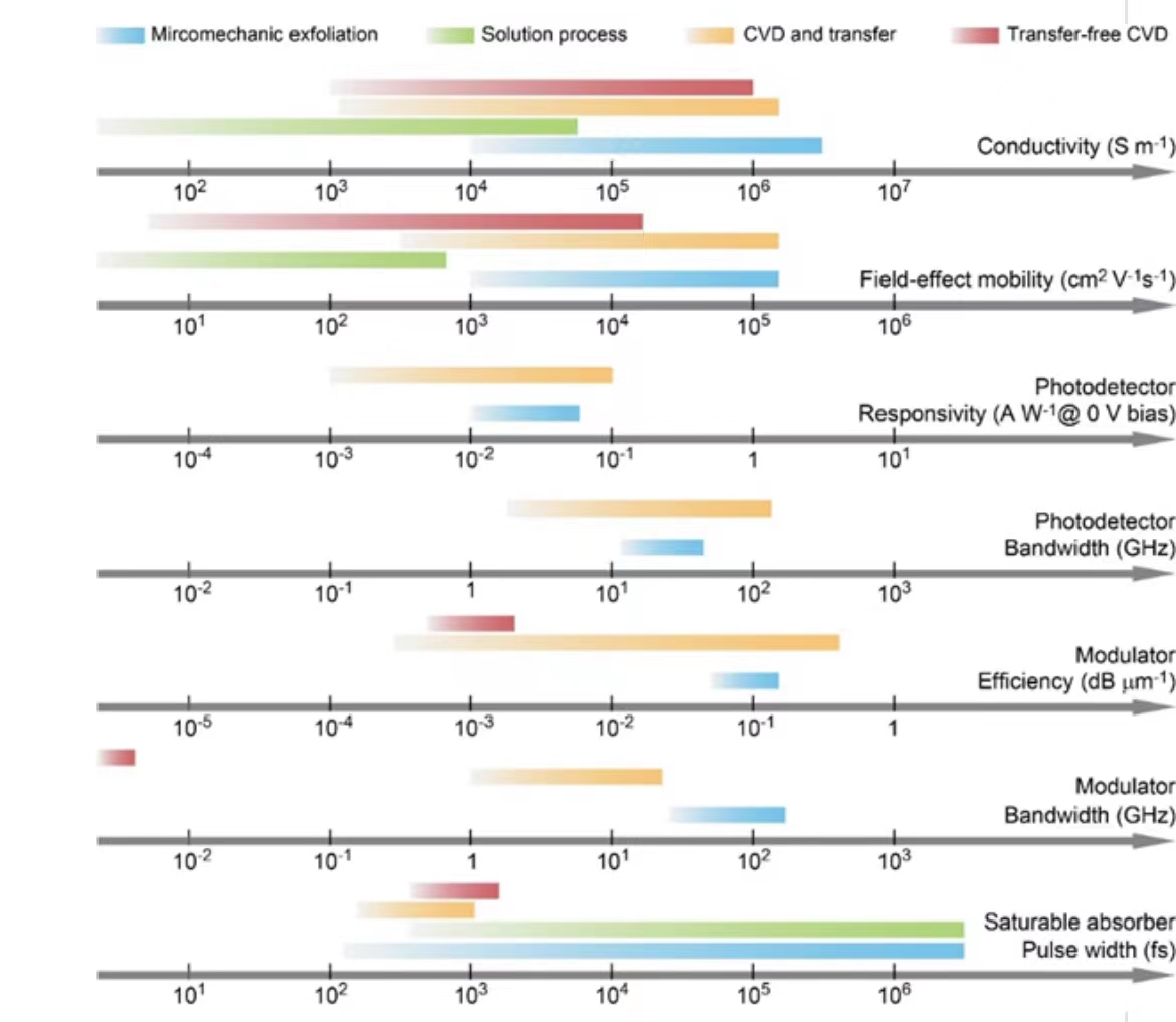
The large-scale manufacture of high-quality GIWGs is the key to the practical application of GIWGs photonic devices. In this paper, the effects of different preparation processes on graphene material quality and device performance are compared.The research progress of GIWGs in detectors, modulators, ultrafast lasers, nonlinear optics and biosensing is briefly summarized.

Figure 3. Preparation method of GIWGs

Figure 4: Performance comparison of GIWGs prepared by different methods and devices
Finally, the author makes a summary and outlook. GIWGs, as the most competitive graphene optoelectronic components compatible with CMOS in the future, have attracted much attention, but they still face challenges in practical applications.
(1) Preparation of high-quality graphene materials.
(2) Large area, high throughput transfer method of graphene film. The inevitable damage and pollution of graphene in the transfer process will cause the optical loss of graphene to increase, thus reducing the device performance.
(3) Large scale preparation technology compatible with CMOS process.
(4) The inevitable optical loss caused by the intrinsic absorption of graphene.
(5) The balance between high speed and high efficiency of GIWGs devices.
However, various bottlenecks will be broken through with the continuous innovation of graphene preparation technology, device micromachining technology and new principle device models. With the continuous improvement of people's requirements for graphene material quality, device manufacturing accuracy and photoelectric performance, the vigorous development of GIWGs requires continuous and systematic cooperation between academia and industry in the field of data communication and telecommunications.